
By Diana Sandu, Packaging Engineering Manager, Marvell

1. Step Outside Your Comfort Zone
I joined Marvell through the Inphi acquisition back in 2021 during my fourth year of my BSc program. I studied Electrical Engineering and Applied Electronics at the University POLITEHNICA of Bucharest. Before joining, I wasn't familiar with Marvell or any other semiconductor companies, nor did I have any background in packaging design. When a friend of mine, who had previously interned at Marvell, told me about the internship, I decided to apply.
2. Don’t Be Afraid to Try
A few months into the internship, a 6-month program, one of the projects I was working on with two other interns was sold to a client, which meant we then worked on a tight schedule solving challenging technical issues in real time. We were working on a design for 5G communication, using 2.5D Packaging, which includes the interposer. The project taught me so much about layout and packaging design and helped me gain the skills I needed. During the project, I became a full-time employee as a Junior Packaging and Signal Integrity Engineer.
By Michael Arsenault, Director of Product Marketing for AEC DSPs, Marvell
Rack connectivity is undergoing a historic transformation. Data center operators are demanding both scale-up and scale-out connectivity that can move more data across longer distances and between more systems, while delivering unprecedented levels of energy efficiency and reliability.
To help cable providers and their customers meet these challenges, Marvell has launched the Golden Cable initiative, designed to accelerate the development of active electrical cables (AECs). AECs are a rapidly growing class of high-bandwidth, enhanced copper interconnects used to link servers, switches, NICs and other assets in the same rack or across adjacent racks (about two to nine meters).
The Golden Cable initiative delivers a validated cable architecture tested across leading platforms and built on industry-leading software, reference designs, technical data, firmware and comprehensive support. Participants can combine these assets with their own technology to develop unique AECs powered by DSPs, optimized for specific customer requirements and use cases.
To further enhance performance and ensure broad compatibility, Golden Cable AECs are rigorously tested in the Marvell Cloud Interoperability Lab. Here, cables are validated across a wide range of customized configuration scenarios involving leading XPUs, CPUs, NICs, servers, switches, optical modules and other critical infrastructure components. This process enables Marvell and its partners to validate AEC firmware before cables reach end-customers, significantly accelerating customer qualification and deployment timelines. The result is greater confidence from the first plug-in.
By Vienna Alexander, Marketing Content Professional, Marvell

In a recent Forbes and Statista ranking, Marvell was named as one of America’s Best Midsize Employers for 2026.
The America’s Best Employers ranking, now in its eleventh year, recognizes organizations that have demonstrated an outstanding commitment to fostering collaborative workplaces. To present the ranking, Forbes partnered with established market research firm Statista.
The list is based on over 217,000 U.S. employee independent survey responses from companies with a national workforce of at least 1,000 people. To further categorize the results, companies with between 1,000 and 5,000 employees were deemed midsized, while companies with more than 5,000 people were referred to as large employers. The survey evaluates areas of Atmosphere and Development; Salary and Wage; Company Image; Culture; Working Conditions; and Workplace Environment.
By Alua Suleimenova, Senior Sustainability Program Manager, Marvell

This blog was originally posted in Semiconductor Engineering.
The semiconductor industry is the bedrock of modern technology, enabling everything from AI and cloud computing to electric vehicles. Yet, this critical sector is also one of the most resource-intensive globally, with a substantial dependency on water. A single fabrication plant can demand up to 10 million gallons of water daily, comparable to the consumption of a city with 300,000 residents. Much of this water is, of course, reused and recycled through sophisticated systems. This immense water usage, particularly the requirement for ultrapure water for processes like cleaning and etching, makes consistent access to high-quality water a non-negotiable for operational reliability and business continuity. The new insights report “Ripple Effects: Water Risk and Resilience Across the Semiconductor Value Chain” provides the first global baseline of water risk hotspots for the semiconductor sector, assessing water risks across 140 facilities across 89 water basins to inform future risk mitigation strategies.
By Khurram Malik, Senior Director of Marketing, Custom Cloud Solutions, Marvell
Can AI beat a human at the game of twenty questions? Yes.
And can a server enhanced by CXL beat an AI server without it? Yes, and by a wide margin.
While CXL technology was originally developed for general-purpose cloud servers, the technology is now finding a home in AI as a vehicle for economically and efficiently boosting the performance of AI infrastructure. To this end, Marvell has been conducting benchmark tests on different AI use cases.
In December, Marvell, Samsung and Liqid showed how Marvell® StructeraTM A CXL compute accelerators can reduce the time required for conducting vector searches (for analyzing unstructured data within documents) by more than 5x.
In February, Marvell showed how a trio of Structera A CXL compute accelerators can process more queries per second than a cutting-edge server CPU and at a lower latency while leaving the host CPU open for different computing tasks.
Today, this blog post will show how Structera CXL memory expanders can boost performance of inference tasks.
AI and Memory Expansion
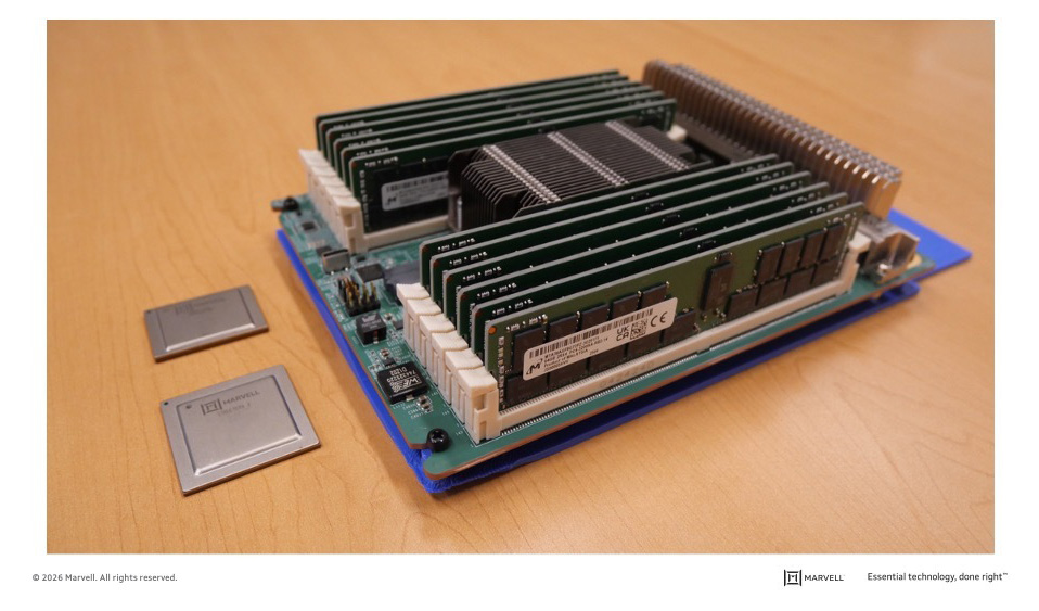
Unlike CXL compute accelerators, CXL memory expanders do not contain additional processing cores for near-memory computing. Instead, they supersize memory capacity and bandwidth. Marvell Structera X, released last year, provides a path for adding up to 4TB of DDR5 DRAM or 6TB of DDR4 DRAM to servers (12TB with integrated LZ4 compression) along with 200GB/second of additional bandwidth. Multiple Structera X modules, moreover, can be added to a single server; CXL modules slot into PCIe ports rather than the more limited DIMM slots used for memory.

Copyright © 2026 Marvell, All rights reserved.