
By Khurram Malik, Senior Director of Marketing, Custom Cloud Solutions, Marvell
Can AI beat a human at the game of twenty questions? Yes.
And can a server enhanced by CXL beat an AI server without it? Yes, and by a wide margin.
While CXL technology was originally developed for general-purpose cloud servers, the technology is now finding a home in AI as a vehicle for economically and efficiently boosting the performance of AI infrastructure. To this end, Marvell has been conducting benchmark tests on different AI use cases.
In December, Marvell, Samsung and Liqid showed how Marvell® StructeraTM A CXL compute accelerators can reduce the time required for conducting vector searches (for analyzing unstructured data within documents) by more than 5x.
In February, Marvell showed how a trio of Structera A CXL compute accelerators can process more queries per second than a cutting-edge server CPU and at a lower latency while leaving the host CPU open for different computing tasks.
Today, this blog post will show how Structera CXL memory expanders can boost performance of inference tasks.
AI and Memory Expansion
Unlike CXL compute accelerators, CXL memory expanders do not contain additional processing cores for near-memory computing. Instead, they supersize memory capacity and bandwidth. Marvell Structera X, released last year, provides a path for adding up to 4TB of DDR5 DRAM or 6TB of DDR4 DRAM to servers (12TB with integrated LZ4 compression) along with 200GB/second of additional bandwidth. Multiple Structera X modules, moreover, can be added to a single server; CXL modules slot into PCIe ports rather than the more limited DIMM slots used for memory.

By Khurram Malik, Senior Director of Marketing, Custom Cloud Solutions, Marvell
While CXL technology was originally developed for general-purpose cloud servers, it is now emerging as a key enabler for boosting the performance and ROI of AI infrastructure.
The logic is straightforward. Training and inference require rapid access to massive amounts of data. However, the memory channels on today’s XPUs and CPUs struggle to keep pace, creating the so-called “memory wall” that slows processing. CXL breaks this bottleneck by leveraging available PCIe ports to deliver additional memory bandwidth, expand memory capacity and, in some cases, integrate near-memory processors. As an added advantage, CXL provides these benefits at a lower cost and lower power profile than the usual way of adding more processors.
To showcase these benefits, Marvell conducted benchmark tests across multiple use cases to demonstrate how CXL technology can elevate AI performance.
In December, Marvell and its partners showed how Marvell® StructeraTM A CXL compute accelerators can reduce the time required for vector searches used to analyze unstructured data within documents by more than 5x.
Here’s another one: CXL is deployed to lower latency.
Lower Latency? Through CXL?
At first glance, lower latency and CXL might seem contradictory. Memory connected through a CXL device sits farther from the processor than memory connected via local memory channels. With standard CXL devices, this typically results in higher latency between CXL memory and the primary processor.

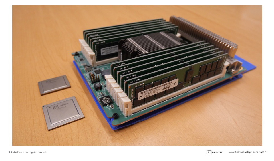
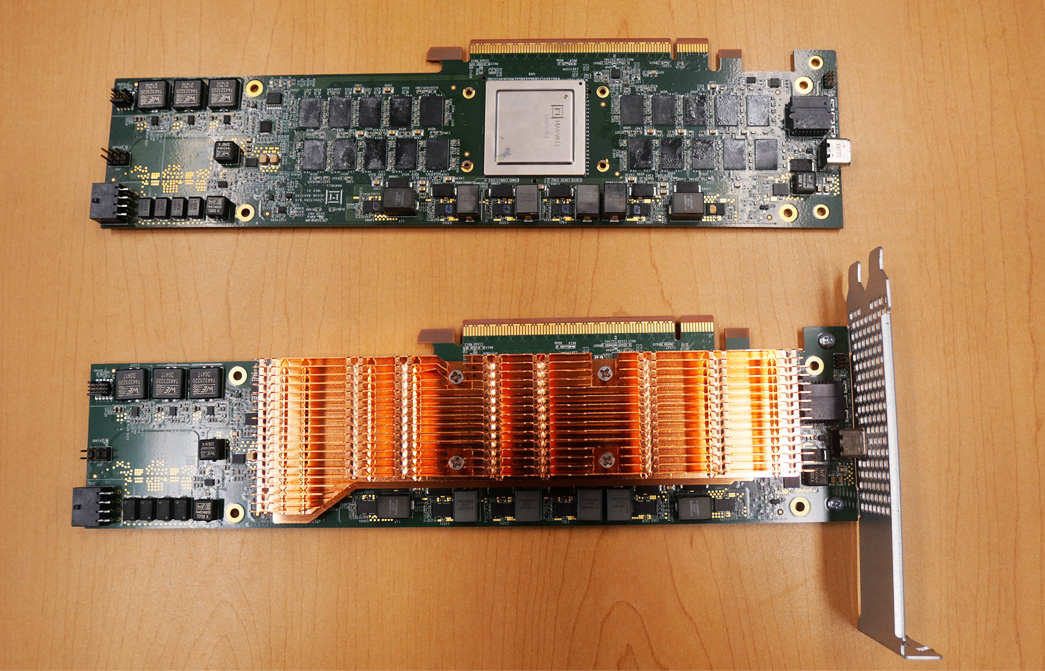
Marvell Structera A CXL memory accelerator boards with and without heat sinks.
By Chander Chadha, Director of Marketing, Flash Storage Products, Marvell
AI is all about dichotomies. Distinct computing architectures and processors have been developed for training and inference workloads. In the past two years, scale-up and scale-out networks have emerged.
Soon, the same will happen in storage.
The AI infrastructure need is prompting storage companies to develop SSDs, controllers, NAND and other technologies fine-tuned to support GPUs—with an emphasis on higher IOPS (input/output operations per second) for AI inference—that will be fundamentally different from those for CPU-connected drives where latency and capacity are the bigger focus points. This drive bifurcation also likely won’t be the last; expect to also see drives optimized for training or inference.
As in other technology markets, the changes are being driven by the rapid growth of AI and the equally rapidly growing need to boost the performance, efficiency and TCO of AI infrastructure. The total amount of SSD capacity inside data centers is expected to double to approximately 2 zettabytes by 2028 with the growth primary fueled by AI.1 By that year, SSDs will account for 41% of the installed base of data center drives, up from 25% in 2023.1
Greater storage capacity, however, also potentially means more storage network complexity, latency, and storage management overhead. It also means potentially more power. In 2023, SSDs accounted for 4 terawatt hours of data center power, or around 25% of the 16 TWh consumed by storage. By 2028, SSDs are slated to account for 11TWh, or 50%, of storage’s expected total for the year.1 While storage represents less than five percent of total data power consumption, the total remains large and provides incentives for saving. Reducing storage power by even 1 TWh, or less than 10%, would save enough electricity to power 90,000 US homes for a year.2 Finding the precise balance between capacity, speed, power and cost will be critical for both AI data center operators and customers. Creating different categories of technologies becomes the first step toward optimizing products in a way that will be scalable.
By Winnie Wu, Senior Director Product Marketing at Marvell
Welcome to the beginning of row-scale computing.
At the 2025 OCP Global Summit, Marvell and Infraeo will showcase a breakthrough in high-speed interconnect technology — a 9-meter active electrical cable (AEC) capable of transmitting 800G across standard copper. The demonstration will take place in the Marvell booth #B1.
This latest innovation brings data center architecture one step closer to full row-scale AI system design, allowing copper connections that stretch across seven racks - that’s nearly the length of a standard 10-rack row. It builds on the prior achievement by Marvell of a 7-meter AEC demonstrated at OFC 2025, pushing high-speed copper technology even further beyond what was thought possible.
Pushing the Boundaries of Copper
Until now, copper connections in large-scale AI systems have been limited by reach. Traditional electrical cables lose signal quality as distance increases, restricting system architects to a few meters between servers or racks. The 9-meter AEC changes that equation.
By combining high-performance digital signal processing (DSP) with advanced noise reduction and signal integrity engineering, the new design extends copper’s effective range well beyond conventional limits, maintaining clean, low-latency data transfer over distances once thought achievable only with optical fiber.
By Annie Liao, Product Management Director, ODSP Marketing, Marvell
For over 20 years, PCIe, or Peripheral Component Interconnect Express, has been the dominant standard to connect processors, NICs, drives and other components within servers thanks to the low latency and high bandwidth of the protocol as well as the growing expertise around PCIe across the technology ecosystem. It will also play a leading role in defining the next generation of computing systems for AI through increases in performance and combining PCIe with optics.
Here’s why:
PCIe Transitions Are Accelerating
Seven years passed between the debut of PCIe Gen 3 (8 gigatransfers/second—GT/s) in 2010 and the release of PCIe Gen 4 (16 GT/sec) in 2017.1 Commercial adoption, meanwhile, took closer to a full decade2

Toward a terabit (per second): PCIe standards are being developed and adopted at a faster rate to keep up with the chip-to-chip interconnect speeds needed by system designers.